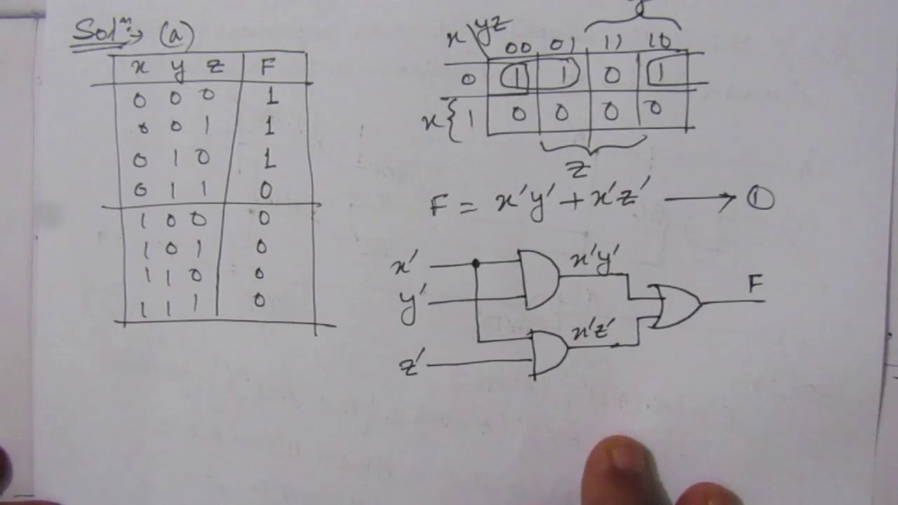
Design A Combinational Circuit That Generates Output As 1 Only For Particular Input Pattern
Q 4 4 Design A Combinational Circuit With Three Inputs And One Output A The Output Is 1 When Youtube
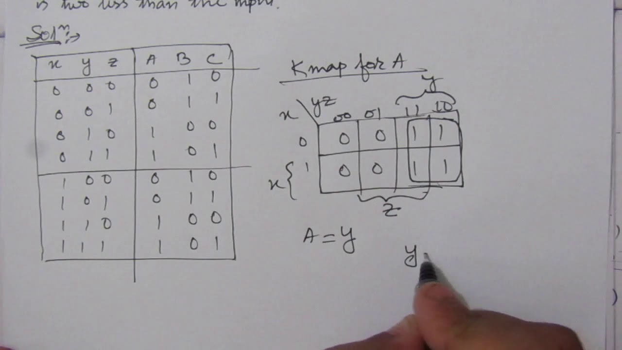
Q 4 5 Design A Combinational Circuit With Three Inputs X Y And Z And Three Outputs A B And C Youtube
Https Ece Uwaterloo Ca Msachdev Ece223 Assignment4 Solution 3rd Edition Pdf
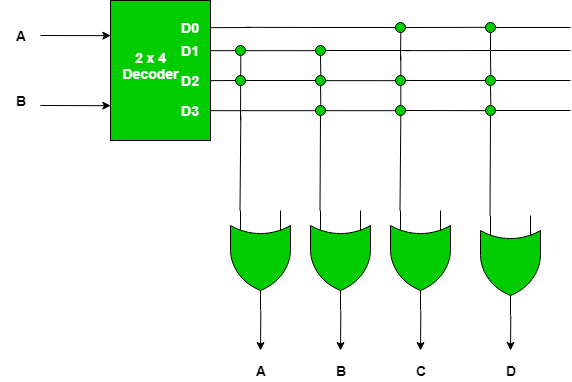
Combinational Circuits Using Decoder Geeksforgeeks

4 1 Annotated Slides 4 Combinational Logic Computation Structures Electrical Engineering And Computer Science Mit Opencourseware

Priority Encoder And Digital Encoder Tutorial

These functions can be described using logic expressions but is most often at least initially using truth tables.
Design a combinational circuit that generates output as 1 only for particular input pattern.
Https Ece Uwaterloo Ca Cgebotys New Quizzes Extratutorialans Pdf

Combinational Logic Circuits Using Logic Gates
Http Web4 Uwindsor Ca Users A Alginahi 60 265 Nsf 831fc2c71873e46285256d6e006c367a 9391445fba4fc83f85256fc8004827a3 File Assignment3 Solutions 20265 Pdf

Tn528i6rzbsbkm

Sequential Logic Circuits Circuit Digital Circuit Logic
Http Www Ee Ic Ac Uk Pcheung Teaching De1 Ee Lectures Lecture 2011 20 20logic 20gates 20and 20boolean 20 X2 Pdf
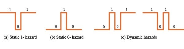
Hazards In Combinational Logic Technical Articles
5 Logic Circuits

Signal Processing Fundamentals Signal Processing Compressor Fundamental
Classification And Programming Of Read Only Memory Rom Geeksforgeeks

Combinational Circuit An Overview Sciencedirect Topics

Moore Machine An Overview Sciencedirect Topics

Conversion Of Flip Flops From One Flip Flop To Another

Ask Modulator Circuit Diagram Circuit Diagram Modulators Circuit
Design 101 Sequence Detector Mealy Machine Geeksforgeeks

Sequential Circuits An Overview Sciencedirect Topics

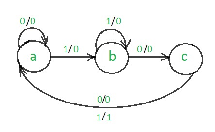
State Diagrams And State Tables

7 Finite State Machine Fpga Designs With Verilog And Systemverilog Documentation
Https Encrypted Tbn0 Gstatic Com Images Q Tbn 3aand9gcszd58ubycdw G3exhx8g9ezn9pqne01jz7kuwquuxzodjbsk7u Usqp Cau

Synchronous Sequential Circuit An Overview Sciencedirect Topics

Logic Circuits An Overview Sciencedirect Topics

Rectification Of A Three Phase Supply Using Diodes
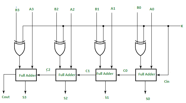
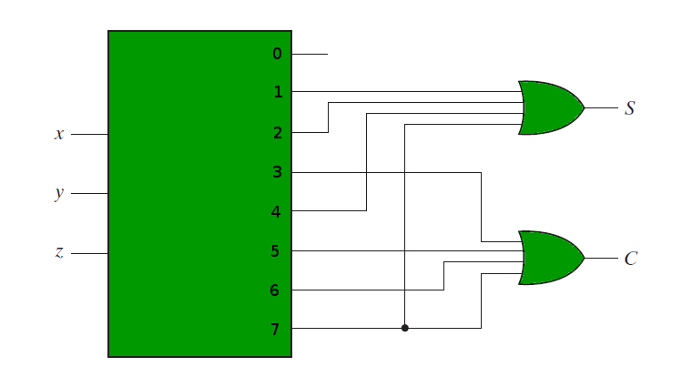
4 Bit Binary Adder Subtractor Geeksforgeeks
Vlsi Design Quick Guide Tutorialspoint
Source : pinterest.com
